Microstrip Impedance Calculator Formula
Z₀ = (60 / √ε_eff) × ln(8H / W_eff + 0.25 × W_eff / H) for W/H ≤ 1
Z₀ = (120π) / [√ε_eff × (W_eff/H + 1.393 + 0.667 × ln(W_eff/H + 1.444))] for W/H ≥ 1
Where the effective permittivity is given by:
ε_eff = (ε_r + 1)/2 + (ε_r – 1)/2 × [1/√(1 + 12H/W_eff) + 0.04(1 – W_eff/H)²]
Formula Explanation
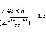
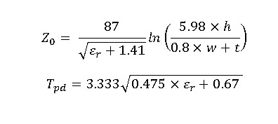
The Microstrip Impedance Calculator determines the characteristic impedance (Z₀) of a PCB trace based on its geometry and the dielectric material used. The formula uses the Hammerstad model for effective permittivity (ε_eff) and applies thickness correction for accurate width calculation (W_eff). The impedance depends on the width (W), dielectric height (H), trace thickness (t), and the dielectric constant (ε_r) of the material. It also estimates propagation delay using the dielectric constant and the speed of light.
Uses of Microstrip Impedance Calculator
The Microstrip Impedance conversion calculator is commonly used in the following applications:
- Designing high-frequency printed circuit boards (PCBs).
- Matching impedance for RF and microwave transmission lines.
- Optimizing trace geometry for signal integrity in high-speed circuits.
- Educational and research use in studying microstrip transmission theory.
- Validating design parameters before PCB manufacturing.
Formula Example
Example calculation using the Microstrip Impedance Calculator:
Let W = 2 mm, H = 1 mm, t = 0.035 mm, and ε_r = 4.4.
Then W/H = 2, which means we use the second equation:
Z₀ = (120π) / [√ε_eff × (2 + 1.393 + 0.667 × ln(2 + 1.444))]
After calculating ε_eff ≈ 3.33, the impedance is approximately Z₀ ≈ 52.8 Ω.
This result shows that the microstrip line will have a characteristic impedance close to 50 Ω, which is ideal for most RF designs.